
Exporatory Devices
In our effort in nanoscale devices we develop and fabricate “exploratory structures” that are specifically designed to harness the novel physical principles found in nanoscale materials. We use these exploratory devices to elucidate key interfacial phenomena endemic to sequential increases in complexity, e.g., in progressing from an individual nanocrystal to a small molecular-like assembly and finally to an extended array of nanoparticles. We are also exploring new approaches for electronic coupling on colloidal nanoparticles to traditional thin-film structures such as quantum wells. The focus of our device-oriented work is on materials and structures amenable to scalable, low-cost fabrication and processing methodologies, such as solution-based synthesis, and on the development and refinement of compatible new physical growth techniques. Some specific topics of our research in the device area include nanocrystal lasing using concepts of single-exciton optical gain, new approaches to LEDs based on “noncontact pumping” from a proximal quantum well, “all-inorganic” LED architectures where nanocrystals are encapsulation at p-n junctions formed by two inorganic layers, energy-transfer solar cells and hybrid photovotaics using nanocrystals coupled to thin semiconductors layers. Our device work typically requires an integrated approach where each study involves materials synthesis, device assembly, and both advanced spectroscopic and detailed electronic characterization.
Our device work is primarily conducted in a dedicated class 10,000 clean room containing facilities specifically designed to handle colloidal nanocrystals and equipped with several systems for thin film growth using thermal evaporation and magnetron sputtering. The clean-room facility is co-located with high-resolution transmission electron microscope (JEOL 2010 TEM with silicon drift detector EDS, w/ Peltier cooling, by Bruker AXS).
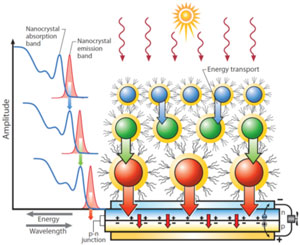
A concept on the “energy-transfer” solar cell. A sequence of nanocrystal layers, with sequentially larger quantum dots. The top layer, the smallest quantum dots, will absorb, say, a blue photon, and create an exciton. The exciton is transferred to sequentially larger quantum dots through a two-step process of decay and excitation (represented by arrows) and then to the p-n junction. There the electric field splits the exciton into an electron and a hole that travel to different terminals. This process avoids charge hopping.