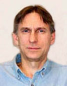
Don Werder

Phone: 505-667-0022
Email: dwerder@lanl.gov
Professional Career
- 2003 - present: Technical Staff Member, Los Alamos National Laboratory, Los Alamos, NM
- 1985 - 2002: Member of Technical Staff, Bell Laboratories, Murray Hill, NJ
- 1981 - 1985: Senior Technical Associate, Bell Laboratories, Murray Hill, NJ
Education
- 1985: MS, Materials Science, Stevens Institute of Technology, Hoboken, NJ
- 1981: BS, Chemical Physics, Rutgers University, New Brunswick, NJ
Current Research
- Characterization of phase, structure and composition of nanoscale materials by transmission electron microscopy and scanning transmission electron microscopy.
- Fabrication and characterization of nanoscale-based devices.
- Thin-film deposition by thermal evaporation and RF magnetron sputtering.
- I am also the person in charge of the TEM and cleanroom facilities. I am presently constructing a dedicated device characterization lab.
Previous Research
- Photolithography, metrology and molecular beam epitaxy of InP-based, high-speed, bipolar transistors.
- Transmission electron microscopy of high-temperature superconductors.
- Studies of oxygen vacancy ordering in YBaCuO.
- Transmission electron microscopy studies in the development of new bonding metals for flip-chip technologies. Studies of meta-stable alloy phases.
- Transmission electron microscopy studies for the development alternative gate oxides.
- Scanning transmission electron microscopy/molecular beam epitaxy in-situ studies of strained layer epitaxy.
- Transmission electron microscopy studies of AlGaAs/GaAs quantum wells fabricated by ion-implantation and diffusion.
- Reflection electron microscopy studies of disorder in the contact resistance of oxidized Ni and Ni-Sb films.
- Development of plasma etching process of GaAs-based lasers produced by proton bombardment.
August 2010
